
Green gold deposition process for multi-layer PCB circuit boards, high-density interconnects, HDI precision electronic circuit board sampling in bulk
Category:
electron/PCB circuit board/PCB circuit board
Model:
PCB circuit board
Brand:
PCB circuit board
Substrate material:
FR-4 epoxy glass fiber
surface treatment:
Sinking Gold (ENIG)
Number of layers in the board:
Multi layer (4-12 layers optional)
copper foil thickness:
1/2oz - 2oz
minimum line width:
3mil (0.076mm)
minimum line spacing:
3mil (0.076mm)
impedance control:
±10%
fire rating:
UL94-V0
Operating Temperature:
-40℃ ~ +130℃
application field:
Communication/Industrial Control/Medical/Automotive Electronics
Retail Price
10,000,000.00USD
重量
kg
- Product Description
-
Substrate material FR-4 epoxy glass fiber
surface treatment Sinking Gold (ENIG)
Number of layers in the board Multi layer (4-12 layers optional)
copper foil thickness 1/2oz - 2oz
minimum line width 3mil (0.076mm)
minimum line spacing 3mil (0.076mm)
impedance control ±10%
fire rating UL94-V0
Operating Temperature -40℃ ~ +130℃
application field Communication/Industrial Control/Medical/Automotive Electronics
Description :
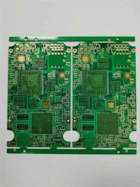
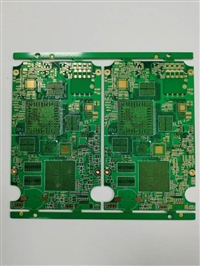
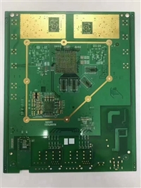
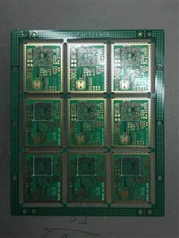
Printed Circuit Board (PCB) is the support body and electrical connection carrier of electronic components. The picture shows a multi-layer high-density interconnect (HDI) circuit board produced using the splicing process. This product is mainly used to solve the problems of signal transmission, power distribution, and component fixation in complex electronic devices. It is typically applied in fields such as communication base stations, industrial control motherboards, medical equipment, and high-performance computers. From the picture, it can be seen that the surface of the PCB board has been finely processed, with dense solder pads and vias, which can effectively carry highly integrated chipsets, ensuring stability and reliability under high-speed signal transmission. It is the fundamental component of modern electronic products.
In terms of specifications and processes, the PCB circuit board substrate usually uses FR-4 epoxy glass fiber cloth laminated board, which has excellent mechanical strength and heat resistance. The surface process adopts immersion gold (ENIG) treatment, and the solder pads are golden yellow in color. Compared with traditional tin spraying process, the immersion gold layer has higher flatness, suitable for soldering fine pitch pins, and has strong oxidation resistance and long storage life. The number of layers of the board is estimated to be 6 or more to meet complex wiring requirements. The execution standard complies with IPC-A-600 Level 2 or Level 3 standards, and the impedance control accuracy is usually within ± 10%. The thickness of copper foil is commonly 1/2oz or 1oz, and the minimum line width/spacing can reach 3mil/3mil. The aperture tolerance is controlled within ± 0.05mm to ensure precise and consistent electrical performance.
When selecting, the number of layers and materials should be determined based on the actual application scenario. For high-frequency and high-speed signal transmission scenarios, such as 5G communication modules, it is necessary to choose high-frequency boards with low dielectric constant (Dk) and low dielectric loss (Df); For ordinary consumer electronics or industrial control equipment, conventional FR-4 material is sufficient to meet the needs. If the pins of the components are densely packed, such as in the BGA packaging area shown in the figure, HDI technology or any layer interconnect technology must be used to ensure the routing channels. Not suitable for simple toy circuits that are extremely cost sensitive and have very low performance requirements. Such scenarios typically use single-sided cardboard or CEM-1 materials. The purchaser should pay attention to distinguishing between rigid boards and flexible boards. The diagram shows a rigid multi-layer board, which is not suitable for parts that require frequent bending.
In terms of installation and maintenance, PCB circuit boards need to be kept dry before surface mount processing. It is recommended to store them in vacuum packaging and bake them to remove moisture before use to prevent board explosion or delamination during reflow soldering. Attention should be paid to temperature curve control during welding to avoid local overheating that may cause pad detachment or substrate carbonization. In daily use, it is necessary to avoid physical impacts that may cause wire breakage, as well as electrochemical migration short circuits caused by humid environments. Common faults include poor contact caused by virtual soldering, circuit burnout or capacitor breakdown caused by overcurrent. During maintenance, obvious defects can be detected through visual inspection or AOI automatic optical inspection. Deep faults require the use of flying needle testing or X-ray fluoroscopy to check the integrity of internal wiring, ensuring long-term stable operation of the equipment.
AfterSalesService :
Key words:
More Products